
Author Affiliations
Abstract
1 School of Physics & State Key Laboratory of Optoelectronic Materials and Technologies, Sun Yat-sen University, Guangzhou 510275, China
2 e-mail: dongjwen@mail.sysu.edu.cn
Second-order topological photonic crystals support localized corner modes that deviate from the conventional bulk-edge correspondence. However, the frequency shift of corner modes spanning the photonic band gap has not been experimentally reported. Here, we observe the gapless corner modes of photonic crystal slabs within a parameter space by considering translation as an additional synthetic dimension. These corner modes, protected by topological pumping in synthetic translation dimensions, are found to exist independently of the specific corner configuration. The gapless corner modes are experimentally imaged via the near-field scanning measurement and validated numerically by full-wave simulations. We propose a topological rainbow with gradient translation, demonstrating the ability to extract and separate specific frequency components of light into different spatial locations. Our work contributes to the advancement of topological photonics and provides valuable insights into the exploration of gapless corner modes in synthetic dimensions.
Photonics Research
2024, 12(3): 444

Author Affiliations
Abstract
1 State Key Laboratory of Optoelectronic Materials and Technologies, Sun Yat-sen University, Guangzhou 510275, China
2 School of Physics, Sun Yat-sen University, Guangzhou 510275, China
In silicon photonics, the cavity mode is a fundamental mechanism to design integrated passive devices for on-chip optical information processing. Recently, the corner state in a second-order topological photonic crystal (PC) rendered a global method to achieve an intrinsic cavity mode. It is crucial to explore such a topological corner state in silicon photonic integrated circuits (PICs) under in-plane excitation. Here, we study both theoretically and experimentally the topological nanophotonic corner state in a silicon-on-insulator PC cavity at a telecommunications wavelength. In theory, the expectation values of a mirror-flip operation for the Bloch modes of a PC slab are used to characterize the topological phase. Derived from topologically distinct bulk polarizations of two types of dielectric-vein PCs, the corner state is induced in a 90-deg-bend interface, localizing at the corner point of real space and the Brillouin zone boundary of reciprocal space. To implement in-plane excitation in an experiment, we fabricate a cross-coupled PC cavity based on the bend interface and directly image the corner state near 1383 nm using a far-field microscope. Finally, by means of the temporal coupled-mode theory, the intrinsic factor of a cross-coupled cavity (about 8000) is retrieved from the measured transmission spectra. This work gives deterministic guidance and potential applications for cavity-mode-based passive devices in silicon PICs, such as optical filters, routers, and multiplexers.
Photonics Research
2021, 9(8): 08001423
Author Affiliations
Abstract
1 School of Physics & State Key Laboratory of Optoelectronic Materials and Technologies, Sun Yat-sen University, Guangzhou 510275, China
2 e-mail: hext9@mail.sysu.edu.cn
3 e-mail: stszfl@mail.sysu.edu.cn
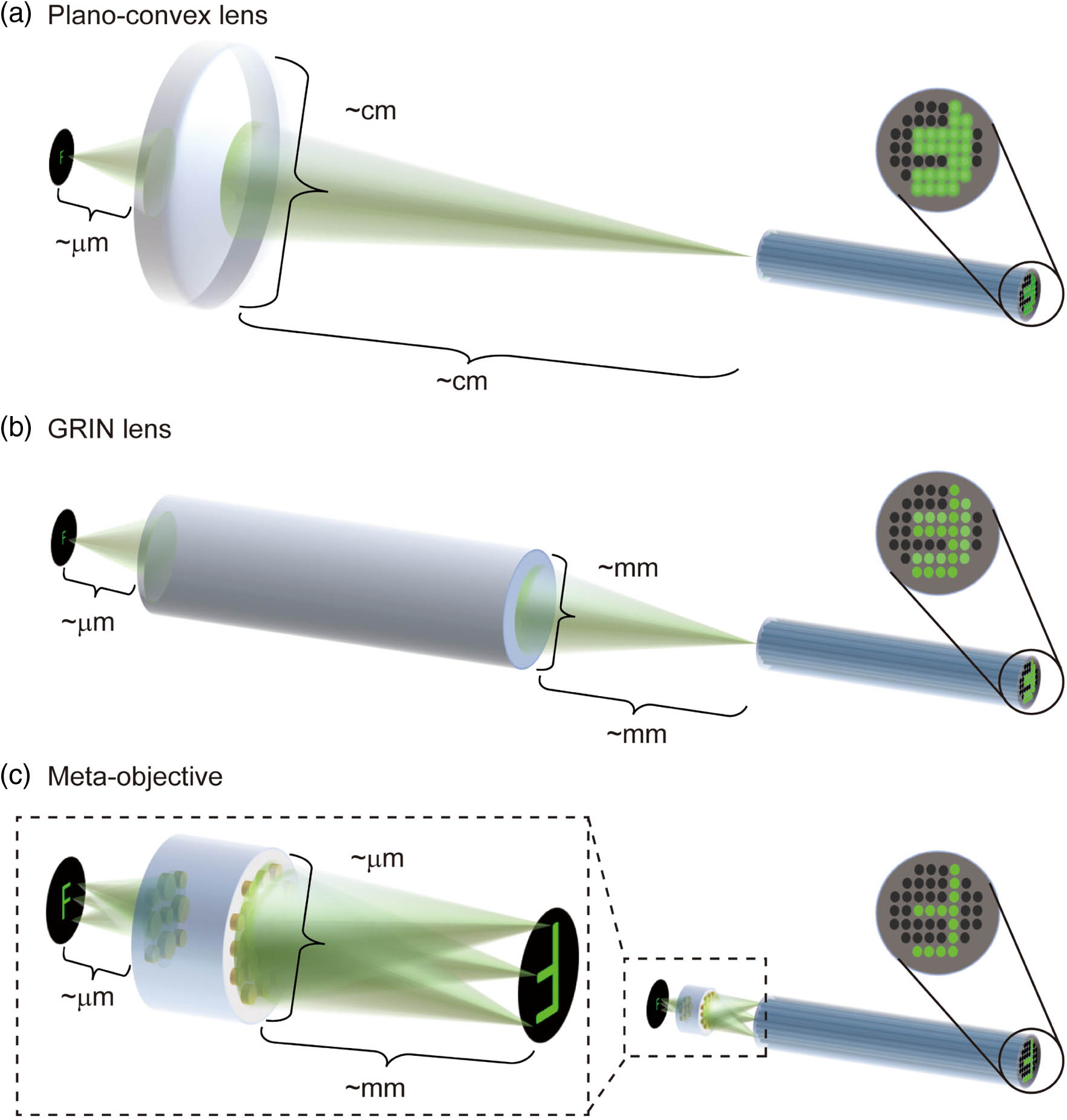
Microendoscopes are vital for disease detection and clinical diagnosis. The essential issue for microendoscopes is to achieve minimally invasive and high-resolution observations of soft tissue structures inside deep body cavities. Obviously, the microscope objective is a must with the capabilities of both high lateral resolution in a wide field of view (FOV) and miniaturization in size. Here, we propose a meta-objective, i.e., microscope objective based on cascaded metalenses. The two metalenses, with the optical diameters of 400 μm and 180 μm, respectively, are mounted on both sides of a 500-μm-thick silica film. Sub-micrometer lateral resolution reaches as high as 775 nm in such a naked meta-objective, with monochromatic aberration correction in a 125 μm full FOV and near diffraction limit imaging. Combined with a fiber bundle microscope system, the single cell contour of biological tissue (e.g., water lily leaf) can be clearly observed, compared to the indistinguishable features in other conventional lens-based fiber bundle systems, such as plano–convex and gradient refractive index (GRIN) cases.
Photonics Research
2021, 9(2): 02000106
中山大学光电材料与技术国家重点实验室, 广东 广州 510275
通过对两种异质结(金属-光子晶体异质结和光子晶体异质结)进行理论计算发现,由两种高反射材料(如负介电常数材料、光子晶体禁带材料)构成的异质结中,存在高透射的局域界面模,并且这种局域界面模的存在与零阻抗条件相关。同时,实验制作了一种金属-光子晶体异质结结构,并在近红外波段观察到该局域界面模的存在。
文字间用 号隔开空半格界面模 零阻抗 光子晶体 奇异材料 异质结 interface mode impedance photonic crystal heterostructure


